• 3 min read
Intel puts High-NA EUV into chip mass production
Intel is using High-NA EUV in mass production of selected Panther Lake chip layers, marking the technology’s first commercial manufacturing deployment.
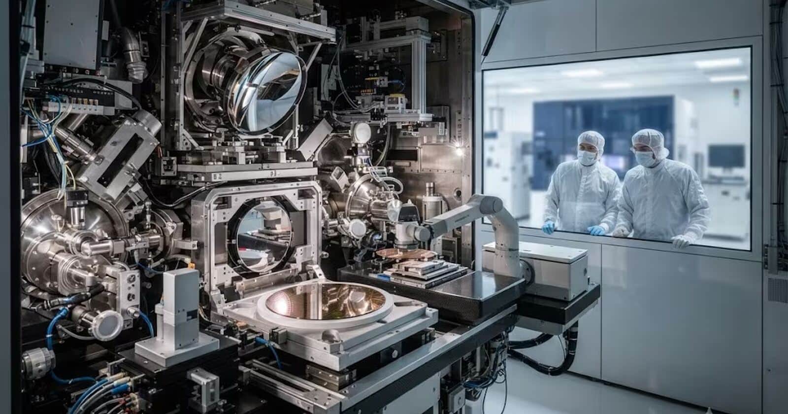
Image: ITzine
Intel has begun serial production using High-NA EUV lithography for selected layers of its Panther Lake processors, which will be sold under the Intel Core Ultra Series 3 brand. It is the first reported case in which high-numerical-aperture EUV has moved beyond test wafers and into the mass production of commercial chips.
The technology is not yet being used across the entire die. Intel has qualified two manufacturing routes for the relevant layers: established NXE systems and ASML’s newer EXE machines. Maintaining both options gives Intel a fallback if production volumes or yields on the new equipment develop more slowly than expected.
High-NA EUV’s resolution and cost
The key change is optical. High-NA EUV systems have a numerical aperture of 0.55, compared with 0.33 for current EUV equipment. ASML says the optical design can improve resolution from 13 nm to 8 nm. Those figures describe the capability of the optics, not a new process-node label for marketing tables.
According to Reuters, a single High-NA EUV machine costs approximately $400 million—almost twice the price of a conventional EUV system. The equipment purchase is only part of the investment. Manufacturers also need to adapt photoresists, photomasks, metrology tools and the broader process-control chain. In practice, High-NA requires a partial restructuring of the factory rather than a single equipment upgrade.

Recommended reading
Silicon Motion targets PCIe 7.0 SSDs for 2027
The immediate manufacturing benefit is practical: some complex structures can be printed with fewer exposures. That can reduce wafer processing time, material consumption and the risk of alignment errors between layers. At high volumes, those savings affect both production costs and potentially the defect rate.
High-NA is therefore being considered not only as a way to shrink features, but also as a method for simplifying long and expensive process flows. The actual gains will depend on chip architecture and on how consistently the equipment maintains yield in commercial production.
Intel Foundry’s High-NA test case
For Intel, Panther Lake is more than a single product launch. It gives the company a production environment in which to measure High-NA EUV on a serial line rather than a demonstration platform.
That experience is also relevant to Intel Foundry, which is seeking external manufacturing customers in competition with TSMC and Samsung. The sooner Intel can operate the new equipment reliably, the more credible it may appear to customers unwilling to pay experimental prices for production chips.
TSMC and Samsung are assessing their own paths, including how quickly the more complex lithography can pay for itself and how disruptive the supporting factory upgrades will be. High-NA does not eliminate the cost of advanced process nodes, but reducing the number of operations on the most difficult layers could materially improve the economics of large dies.
The next test will be production data, not presentation slides. If Intel maintains Panther Lake volumes and yields on the new equipment, High-NA EUV could move beyond an expensive early experiment and become a routine manufacturing tool. If it cannot, the technology may remain too costly even for the companies that invested first.

Computing Editor
Tomas lives in the terminal. He covers chips, laptops, and operating systems with a focus on performance and efficiency. He reads kernel changelogs the way other people read fiction, and he's always on the hunt for the perfect mechanical keyboard switch. If it processes data, Tomas has an opinion on it.
via ITzine