• 3 min read
Zeiss expands EUV optics production for 2nm chips
Zeiss is adding 25,000 square meters in Oberkochen to expand EUV optics production for ASML’s 2nm and smaller chipmaking systems.
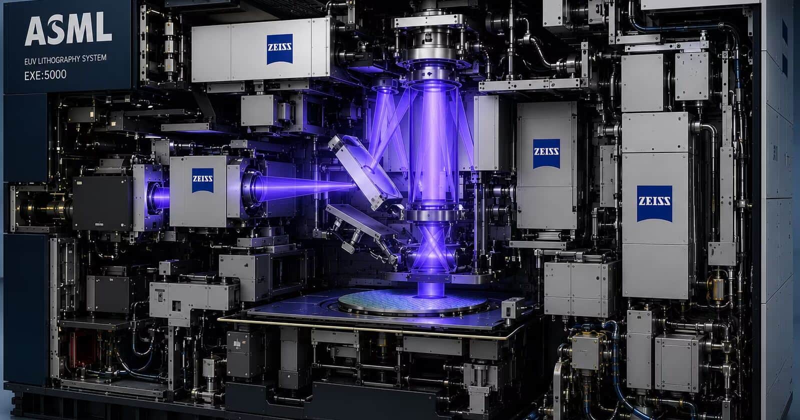
Image: ITzine
Zeiss Semiconductor Manufacturing Technology (Zeiss SMT) is expanding its Oberkochen site by about 25,000 square meters to increase production of the optical systems used in ASML’s lithography machines. Some of the new buildings are already operating; the rest will come online in stages.
The expansion targets a critical constraint in semiconductor manufacturing. ASML’s EUV lithography systems rely on Zeiss optics to produce the most advanced chips, including designs based on 2-nanometer and smaller process nodes. Demand is rising as TSMC, Samsung, and Intel compete for early production capacity on those technologies.
Why ASML depends on Zeiss for 2nm chips
Zeiss’s facilities in Oberkochen and Wetzlar are the only sites in the world that produce the optical columns for ASML’s EUV systems. These are not conventional lenses: they combine mirrors, illumination modules, and other components required for an EUV scanner to operate.

Recommended reading
77% of UK employers want basic AI skills
ASML has acknowledged the dependence in its annual report, stating that its production volume is limited by Zeiss SMT’s capacity. A prolonged disruption in Zeiss supplies would halt the assembly of ASML lithography machines.
ASML therefore finances its partner directly. At the end of 2025, loans issued to Zeiss SMT totaled €1.91 billion, while another €1.19 billion was paid in advance for future deliveries. The arrangement reflects the strategic importance of Zeiss optics to the chip-equipment supply chain.
High-NA EUV raises the production challenge
The next major step is High-NA EUV, ASML’s next-generation lithography platform. It is designed to give chipmakers more flexibility as they continue shrinking transistor features, but it also makes the optics and equipment assembly more complex.
ASML has told investors it plans to increase annual production of Low-NA EUV scanners by about 30% by 2027, from roughly 65 systems per year today. The company has also considered further growth in 2028. At the same time, it is working to reduce assembly time for a lithography system from about 22 weeks to 15–16 weeks.
That faster assembly schedule does not eliminate the key bottleneck: the optical modules still have to be manufactured, tested, and calibrated to extremely tight tolerances. According to Zeiss, a single High-NA EUV optical column contains more than 40,000 parts and weighs about 12 tonnes. Its illumination system adds another 25,000 components and roughly 6 tonnes.
Individual mirrors take months to produce. Final testing takes place in vacuum chambers weighing more than 150 tonnes, with tolerances measured in fractions of a nanometer.
Zeiss SMT’s financial results show how sharply demand has grown. For the year ending in September 2025, the division’s revenue increased 23% to €5.055 billion, making it the largest business in the wider Zeiss Group.
The company is also expanding beyond Oberkochen. It is building another production complex in Wetzlar, enlarging cleanroom facilities in Roßdorf, and has opened an innovation center in South Korea. The struggle for advanced-chip capacity is therefore also a race to expand production of the most constrained part of the EUV supply chain: its precision optics.
Enterprise Editor
Marcus follows the money. He covers enterprise software, cloud architecture, and the tectonic shifts in Big Tech strategy. He translates dense earnings calls and complex M&A activity into actionable insights about where the industry is actually heading. If a tech giant makes a silent pivot, Marcus is usually the first to notice.
via ITzine