• 4 min read
MIT builds 1,000 molecular devices with 96% yield
MIT researchers built over 1,000 molecular devices with 96% yield using self-assembled contacts and sub-nanometer material layers.
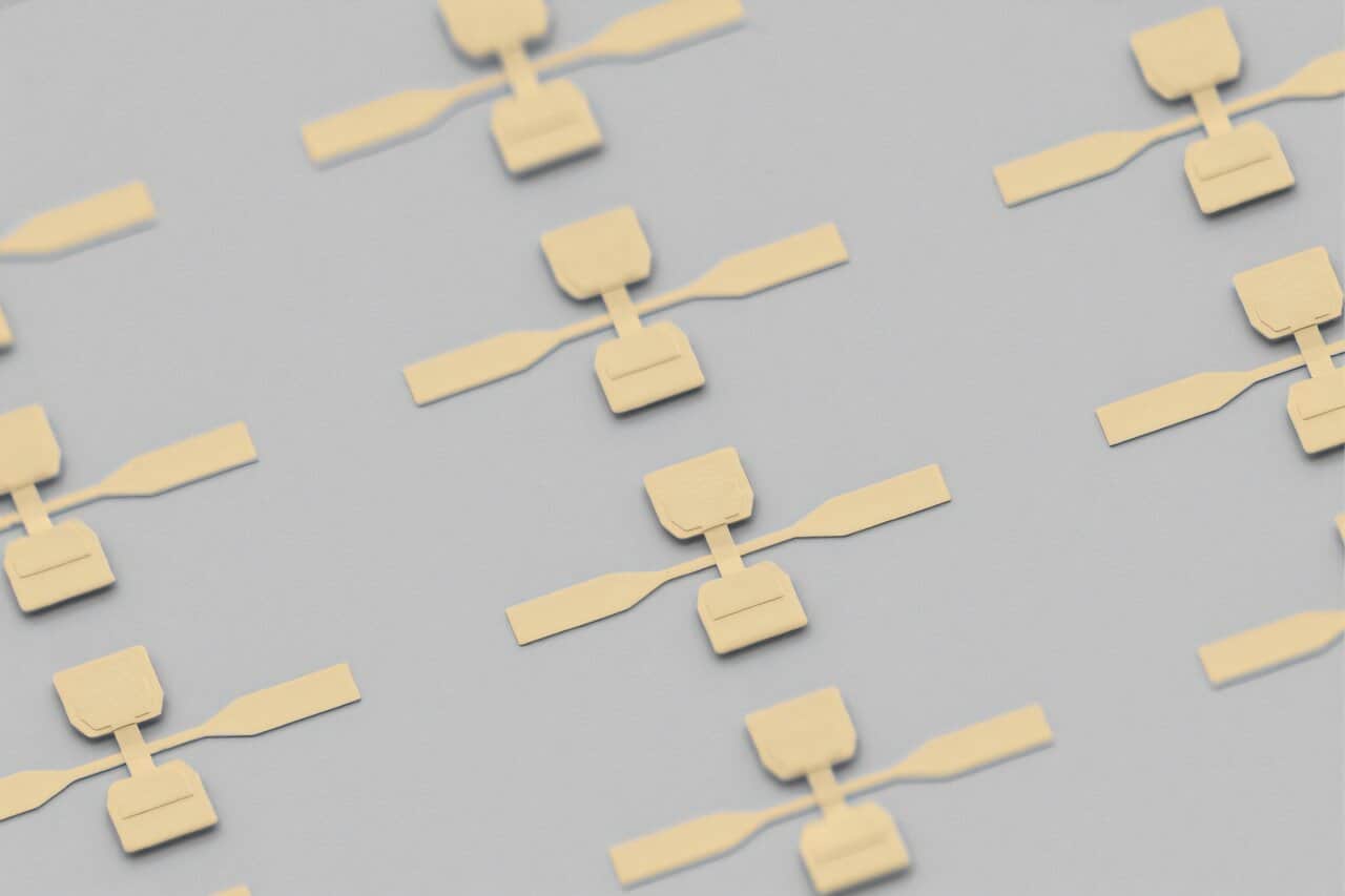
Image: TechXplore
MIT researchers have developed a fabrication platform that integrates fragile molecular materials into electronic devices without exposing them to the damaging chemicals and processing steps used in conventional semiconductor manufacturing.
The team fabricated more than 1,000 devices using molecular layers less than 1 nanometer thick. The devices had an average working yield of 96% and endured tens of thousands of electrical cycles without visible degradation. The work was published in Nature Nanotechnology in 2026.
A two-step process for molecular devices
Molecules are clusters of atoms whose structures and chemistry can be precisely designed. That tunability could support smaller and more adaptable electronics, higher-performance photonic devices, sensing systems and emerging quantum technologies.
The problem is integrating those materials with the other layers required for a functional device. Making electrical contacts typically involves metallic surfaces and manufacturing processes that can damage molecular materials, reducing both reliability and performance.
MIT’s approach separates the conventional fabrication work from molecular integration:

Recommended reading
Rooftop solar changes neighbors' energy choices
- Researchers first fabricate the device components using standard semiconductor processes.
- They deposit the molecular material onto the completed components.
- Nanoscale forces then bring the device structures together, creating an electrical contact without directly processing the molecules with harsh chemicals.
In the demonstration, the team created a scaffold containing two metal electrodes separated by a precisely sized gap. After depositing the molecular layer on the electrode surfaces, the researchers used nanoscale forces to gently pull the top electrode into place, sandwiching the molecules between the contacts.
“By bringing the delicate materials into the process only after we have fabricated the main device elements, it allows us to use conventional processes that are normally not compatible with these nanomaterials.”
How capillary and van der Waals forces assemble the devices
The final structure forms through two nanoscale mechanisms. As the solution containing the molecules evaporates, capillary forces pull the metal surfaces together. The researchers tune the stiffness of the electrodes so that this movement happens gently enough to avoid damaging the molecular layer.
Once the electrodes meet, van der Waals forces help keep the structure stable. By controlling the device’s surface area and the properties of the molecules, the team designed the attraction to hold the electrodes in place without harming the material between them.
“Nanoscale forces play a critical role in our approach. Instead of fabricating exactly the structures we ultimately want, we make something mechanically mobile and use forces to transform it into an architecture that would otherwise be impossible to fabricate.”
The researchers say the technique combines the scalability of conventional semiconductor manufacturing with the precision of self-assembly. Farnaz Niroui, an associate professor of electrical engineering and computer science at MIT, a member of the Research Laboratory of Electronics, and senior author of the paper, described it as a framework for integrating molecules and other nanoscale or quantum materials into functional devices.
“Our platform combines the scalability of conventional semiconductor manufacturing with the precision and control of self-assembly. This establishes a new fabrication framework for the scalable, high-throughput integration of emerging nanoscale and quantum materials, including molecules, into functional devices with architectures and capabilities that were previously infeasible.”
From individual devices to molecular memory arrays
The platform is designed to support circuit- and system-level integration rather than only isolated molecular devices. To demonstrate that capability, the researchers built an interconnected array of molecular memory devices, which they say could be used in next-generation computing platforms.
The process can also be extended to other materials and device architectures. The researchers plan to use it to investigate multifunctional computing and sensing devices and systems, although the source does not specify a commercial product, release date or pricing.
“The stability really stands out. This is a critical feature for moving molecular devices toward practical applications, but it has been a persistent challenge in the field.”
The paper, “Self-assembled contacts for high-yield molecular devices,” was authored by Sarah O. Spector and colleagues and published in Nature Nanotechnology. Its DOI is 10.1038/s41565-026-02227-9. TechXplore republished the story courtesy of MIT News.
Frontier Editor
Dan is our resident futurist, covering electric mobility, space exploration, and the smart home. He's interested in atoms just as much as bits. Whether it's a new battery chemistry, a reusable rocket, or a protocol that finally makes IoT devices talk to each other, Dan breaks down the engineering that pushes humanity forward.
via TechXplore