• 3 min read
HKUST acoustic chip handles 12 times more power
HKUST’s LAW acoustic chip handled 12.73 times more power, cut heat rise 70%, and could support 6G, satellite links, and quantum systems.
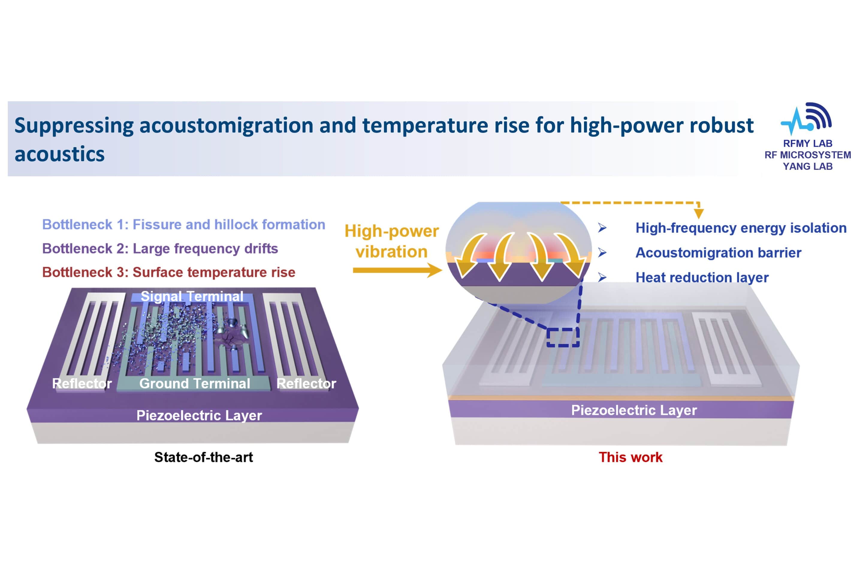
Image: TechXplore
A new acoustic-chip architecture from The Hong Kong University of Science and Technology (HKUST) has handled more than 12 times the power of a state-of-the-art control device while keeping operating temperatures substantially lower.
The platform, called Layered Acoustic Wave (LAW), was tested on transducers vibrating at more than 2 billion times per second. It reduced temperature rise by 70% and reached a record power density of 36.4 W/mm², potentially expanding acoustic chips beyond their traditional role in small-signal filtering.
The research, led by Yansong Yang, assistant professor in HKUST’s Department of Electronic and Computer Engineering, was published in Nature Communications. Fangsheng Qian, Yang’s doctoral student, is the paper’s first author.
Why acoustic chips fail at high power
Acoustic-wave devices convert electromagnetic signals into sound waves at gigahertz frequencies. Their compact size makes them essential to radio-frequency filtering in smartphones and mobile base stations, while newer applications include quantum information, microfluidics, acousto-optics and nonmagnetic energy storage.

Recommended reading
Apple Invites adds emoji reactions and confetti
At high power, however, intense vibration and heat can trigger three related failure mechanisms:
- Metal atoms in electrodes migrate, forming protrusions and voids that can break the circuit.
- Heat changes acoustic velocity, pushing the operating frequency off target.
- Mechanical stress can crack or delaminate the piezoelectric film.
Conventional solutions focus on the underside of the device, often using expensive, thermally conductive substrates such as silicon carbide or diamond. HKUST’s researchers instead redesigned the upper boundary, where heat and stress are concentrated.
How the LAW architecture works
The LAW design places the vibrating surface of a lithium niobate thin-film device beneath a composite boundary: a silicon dioxide isolation layer topped with a thick, amorphous silicon overlayer. The overlayer is much thicker than the acoustic wavelength, yet simulations showed that the acoustic energy remains confined near the surface.
The structure performs three functions simultaneously. It redistributes mechanical stress, reducing peak stress at the electrode interface to about one-quarter of its previous level. It also spreads heat through a material with thermal conductivity roughly two orders of magnitude higher than air, while compensating for thermal expansion to stabilize frequency during temperature changes.
The redesign increased operating frequency by about 25% at a given wavelength and reduced damping loss by about 30%. The team says it can scale across sub-6 GHz bands using standard, low-cost fabrication processes.
Power-test results and potential applications
In component-level tests, the LAW transducer reached a steady-state temperature rise of just 5.2°C, compared with 17.4°C for the thin-film surface acoustic wave (TF-SAW) control device. It tolerated an injected power density of 45.61 dBm/mm², equivalent to 36.4 W/mm²—12.73 times the control threshold—while maintaining a first-order temperature coefficient of frequency of −13 ppm/°C across −150°C to 325°C.
At −85°C, the threshold rose to 49.45 dBm/mm², or 88.11 W/mm², a 13.85-fold increase over the TF-SAW control. The result could be relevant to cryogenic quantum acoustic systems. Failure analysis found severe electrode migration and piezoelectric-film cracking in the control devices, while LAW devices operating at much higher power showed no comparable migration.
“For decades, the community accepted two 'givens': that the surface of an acoustic wave device must stay open to the air, and that high-power operation was far out of reach. We have proven that both assumptions can be broken at the same time.”
The team sees possible applications in direct-to-cell satellite communications, 6G networks, radio-frequency filters, cryogenic quantum acoustic circuits, on-chip acousto-optic and microfluidic systems, and compact nonmagnetic power-conversion modules. The work is described in “Suppressing acoustomigration and temperature rise for high-power robust acoustics,” published in Nature Communications in 2026. DOI: 10.1038/s41467-026-72102-7.

Computing Editor
Tomas lives in the terminal. He covers chips, laptops, and operating systems with a focus on performance and efficiency. He reads kernel changelogs the way other people read fiction, and he's always on the hunt for the perfect mechanical keyboard switch. If it processes data, Tomas has an opinion on it.
via TechXplore