• 4 min read
TSMC maps 2029 chip roadmap with A12, A13, and N2U
TSMC has sketched out its process roadmap through 2029, and the message is pretty clear: smartphones and client devices get yearly refreshes, while AI and HPC get a slower, pricier cadence built around bigger efficiency
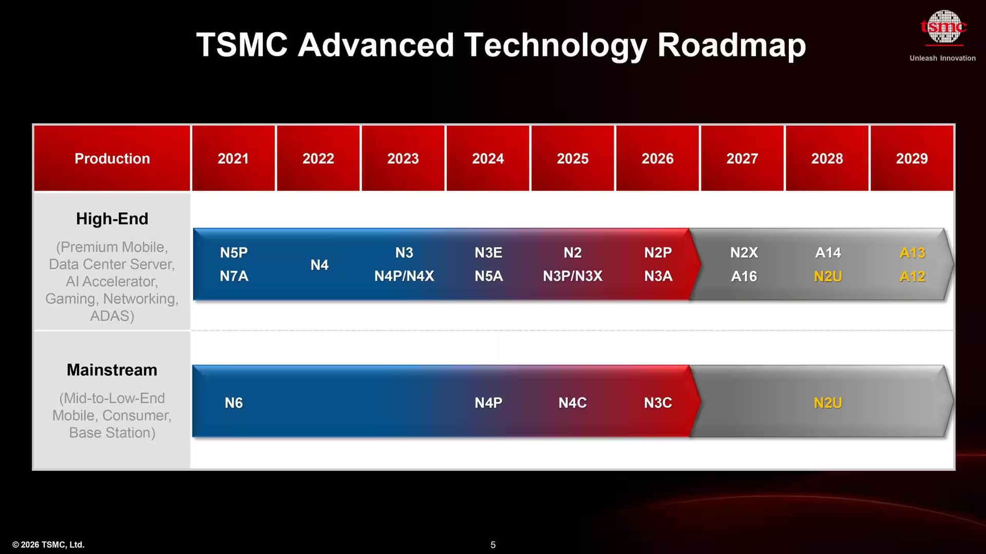
TSMC has sketched out its process roadmap through 2029, and the message is pretty clear: smartphones and client devices get yearly refreshes, while AI and HPC get a slower, pricier cadence built around bigger efficiency jumps. The company also confirmed A12, A13, and N2U, while pushing A16's volume production into 2027 – a small timing shift on paper, but a telling one as chipmakers split their priorities between consumer volume and data-center performance.
If you’re wondering what TSMC’s 2029 chip roadmap actually means, the short answer is this: A13 and N2U are aimed at client chips, while A16 and A12 are built for AI and HPC data centers. TSMC also says A16 volume production has moved to 2027, and neither A13 nor A12 will require High-NA EUV through 2029.
The subtext is the real story. TSMC is no longer pretending that one leading-edge node can serve every customer equally well; it is now openly optimizing for two different business models. That mirrors a broader industry shift, with Nvidia, AMD, and cloud operators all demanding more specialized silicon while handset makers keep obsessing over power and compatibility.
A13 and N2U target client chips
For client applications, TSMC is leaning into continuity rather than drama. A13 is an optical shrink of A14, cutting linear dimensions by about 3% and lifting transistor density by roughly 6% while staying fully compatible with A14 design rules and electrical behavior. That means customers can reuse IP with less pain, which is exactly the sort of boring efficiency silicon buyers love and marketing teams rarely brag about.
N2U does something similar for the N2 family. TSMC says the node should deliver about 3% to 4% higher performance at the same power, or 8% to 10% lower power at the same speed, plus a modest 2% to 3% logic-density gain, while remaining compatible with N2P IP. In practice, that gives chip designers an easier upgrade path for mid-range products without forcing a wholesale redesign.
Recommended reading
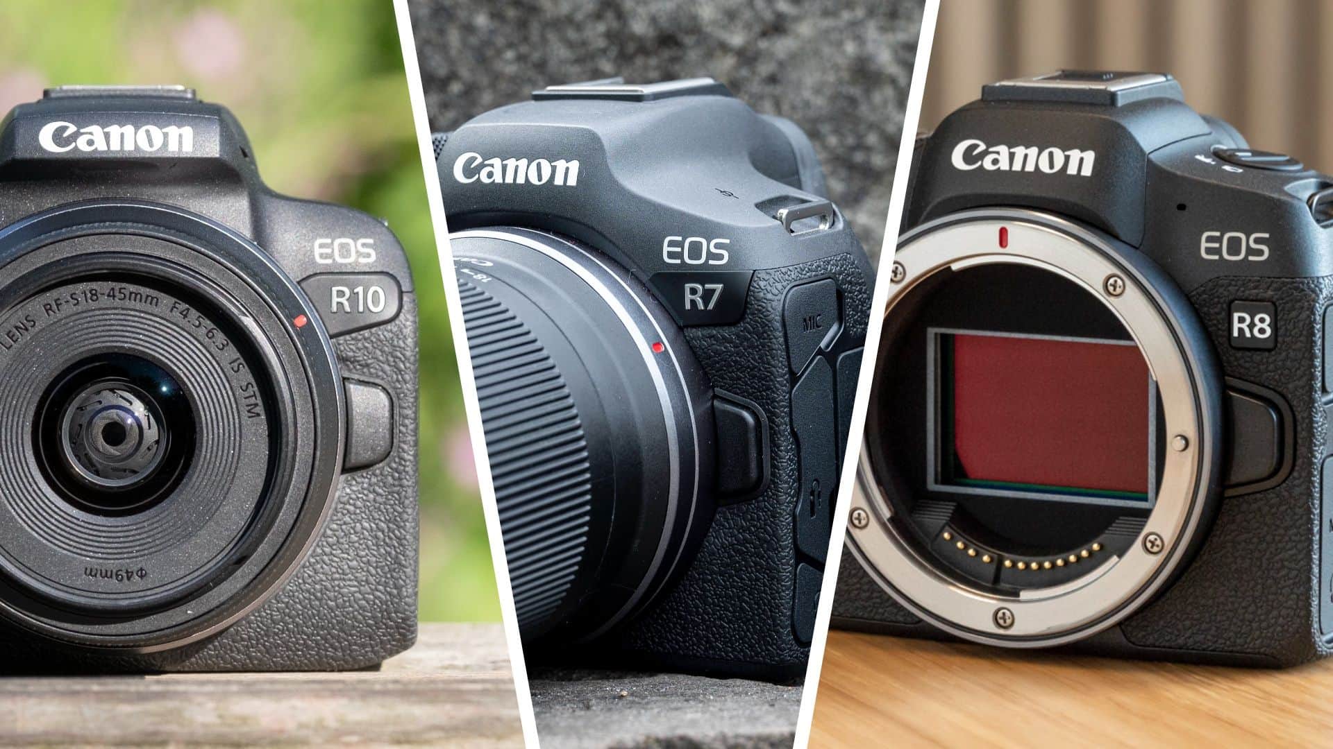
Canon may launch three EOS R cameras in 2026
- A13: about 3% smaller linear dimensions, roughly 6% higher transistor density, production expected in 2029
- N2U: 3% to 4% better performance at the same power, or 8% to 10% lower power at the same speed
- N2U: about 2% to 3% higher logic density, with N2P IP compatibility
A16 and A12 are built for data centers
TSMC’s A16 is the company’s answer to the power-hungry world of AI and HPC, and it is built around Super Power Rail backside power delivery. The node is essentially an N2P-class design with SPR, aimed at delivering better power, performance, and density for data-center workloads where cost takes a back seat to throughput and thermals.
There is also a quiet schedule change here: A16 is now listed as a 2027 technology rather than 2026, even though TSMC says readiness is still on track and the shift reflects customer ramp timing. That is not a scandal, just semiconductor reality. Volume production is decided by the ecosystem, not the slide deck.
A12 is the next step, arriving in 2029 as the successor to A16. TSMC says it will bring full-node gains and continue the move toward backside power delivery improvements, with A13 and A12 both built on A14 and aimed at sharper geometric scaling. The company did not give hard figures, but the direction is obvious: more density, more efficiency, and more specialization for the most expensive chips on the planet.
Why TSMC is avoiding High-NA EUV for now
One of the more pointed details in the roadmap is what TSMC is not using: High-NA EUV lithography. The company says A13 and A12 will not require it through 2029, which is a direct contrast to Intel’s plan to bring High-NA into its 14A generation and beyond. That keeps TSMC on the cheaper side of the technology curve for longer, even as its rival takes the more expensive route in pursuit of node leadership.
That restraint makes sense if you are TSMC. ASML’s High-NA tools are brutally expensive, and if current EUV still delivers the scaling you want, why rush? The answer may change later, but for now TSMC is squeezing more life out of existing lithography while its customers keep paying for better performance per watt.
The next few years should make the split strategy even clearer: consumer chips will keep getting incremental annual upgrades, while data-center parts get the bigger architectural changes and the higher price tags. The open question is how long TSMC can keep extracting those gains without High-NA before the easy wins run out.
Computing Editor
Tomas lives in the terminal. He covers chips, laptops, and operating systems with a focus on performance and efficiency. He reads kernel changelogs the way other people read fiction, and he's always on the hunt for the perfect mechanical keyboard switch. If it processes data, Tomas has an opinion on it.