• 2 min read
Etched hits $10.3 billion valuation for inference chips
Etched reaches a $10.3 billion valuation with SK Hynix backing for custom, low-power AI inference systems.
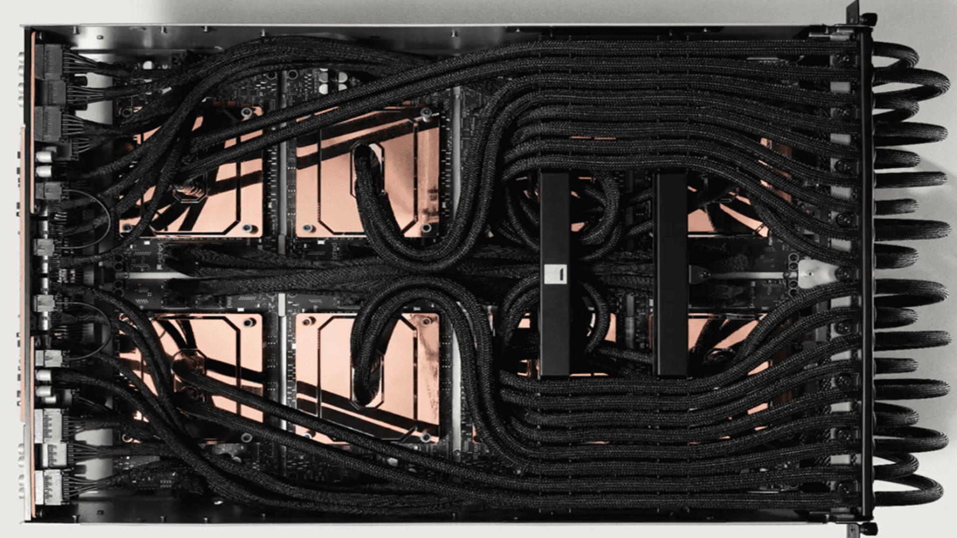
Image: TechRadar
Etched has reached a $10.3 billion valuation after securing new backing from SK Hynix, as the US chip startup prepares to produce rack-scale systems built specifically for AI inference.
The company argues that conventional GPUs often provide more compute than inference workloads need while failing to offer enough memory for increasingly large models. Etched’s alternative combines custom processors, shared memory and lower power consumption instead of relying on general-purpose graphics hardware.
How Etched’s inference architecture works
Founded by former Harvard students Gavin Uberti, Robert Wachen and Chris Zhu, Etched focuses exclusively on inference rather than training large language models. Its systems combine Low Voltage Inference (LVI) with Cluster Scale Memory (CSM), giving processors access to larger shared memory pools than conventional GPUs.
Etched says higher floating-point utilization can increase power draw until thermal limits force a chip to reduce its clock speed. Its architecture is designed to run mathematical processing blocks at less than half the voltage used by most AI chips, which the company says enables several times the FLOPs density of current AI processors.

Recommended reading
MIT study finds AI financial advice works—with caveats
“Today, AI chips can’t scale FLOPs without thermal throttling. As FLOPs utilization increases, AI chips draw more power and downregulate clock speed…”
The company also criticizes the memory tradeoffs in existing hardware. High Bandwidth Memory (HBM) offers capacity, but its memory subsystems and interconnects cannot match the decoding speed of SRAM. Etched’s HBM/SRAM hybrid instead uses a proprietary ultra-low-latency, high-bandwidth interconnect to create a shared memory pool.
“Our HBM/SRAM hybrid design solves both memory capacity and mem2mem latency, enabling high throughput and interactivity simultaneously.”
According to the startup, CSM reduces the time spent moving data among chips, memory and networking hardware by minimizing the number of memory layers involved in transfers. It says the design avoids the cost, reliability, yield, thermal and compute compromises associated with SRAM-only chips, 3D DRAM and optical systems.
Funding and production plans
Etched’s funding has grown rapidly:
- $5.4 million seed round in 2023
- $120 million raised in 2024
- $500 million raised in 2025
- $300 million raised in 2026
The rounds total approximately $925.4 million. The latest financing doubled Etched’s valuation from $5 billion to $10.3 billion. The C-round included Sequoia Capital, Andreessen Horowitz, Jane Street, Diffusion, Argo and SK Hynix.
“This round accelerates production of our inference clusters,” Robert Wachen said. He also confirmed that Etched has opened an 80,000-square-foot, 10 MW facility near Milpitas. The company now employs more than 400 people, reports customer demand exceeding $1 billion, and has manufacturing operations in Taiwan.
Etched says its systems will support conventional large language models, mixture-of-experts architectures and alternatives such as Mamba. The source does not provide pricing or a commercial release date for the systems.
AI Editor
Ava covers the rapidly evolving world of artificial intelligence, from foundational models and research labs to the real-world economics of intelligence. With a background in computational linguistics, she cuts through the hype to find out what actually works. She firmly believes that benchmarks are just marketing until reproduced in the wild.
via TechRadar