TSMC is quietly pulling back from 28-nanometer chips and pushing harder into the parts of the market that pay better: 3 nm, 2 nm, and the coming A14 process. That shift is already opening a lane for rivals such as UMC and VIS, which are built for the mature-node business TSMC is trying to leave behind.
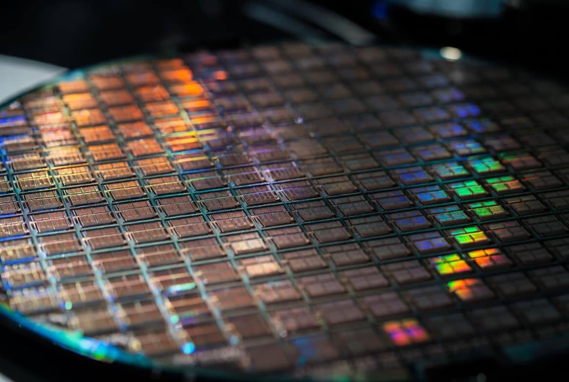
The clearest sign is Fab 15A in Taichung. Since the start of 2026, output there has fallen by about a quarter, from 200,000 to 150,000 silicon wafers a month. The plant has long been one of TSMC’s main 28 nm and 22 nm sites, but the company now wants it converted to 4 nm production while it builds Fab 25 for A14.
Why TSMC is backing away from 28 nm
This is less about abandoning old technology than about chasing the stuff that is suddenly in short supply. AI systems, high-performance computing, servers, and data-center accelerators are eating up advanced capacity, and TSMC is choosing those lines over mature chips because the economics are better and the demand is louder.
There is also a familiar pattern here. Foundries have been squeezing older nodes for years, but the AI boom has made that trade-off harsher: every wafer assigned to a legacy process is one not used for more profitable silicon. TSMC is not alone in prioritizing the newest nodes, but its scale makes the ripple effects much bigger.
What happens to customers still buying mature chips
Analysts say TSMC also plans to move some customers from 28 nm to a more modern 12 nm process. That kind of migration sounds neat on a slide deck, but in practice it means redesign costs, validation time, and a few irritated product managers. Still, it is a sign that the company wants to compress its mature-node business rather than keep expanding it.
- Fab 15A output: about 150,000 wafers a month, down from 200,000.
- Planned future use: 4 nm.
- New capacity in development: Fab 25 for A14.
UMC and VIS are built for exactly this opening
For UMC, the timing is almost gift-wrapped. The company already leans on 28 nm and 22 nm, and it is targeting OLED display drivers, Wi-Fi chips, automotive electronics, and controllers for home appliances and industrial gear. That is the sort of business TSMC is happy to push aside while it pours money into 2 nm, SoIC chiplet packaging, and silicon photonics.
VIS gets a boost, too. TSMC previously handed over some equipment for 200-millimeter wafers, which should help VIS raise output in mature nodes. That matters because the chip industry still needs plenty of non-fancy silicon, even if the headlines are all about AI accelerators and bleeding-edge transistors.
The real fight is over capacity, not technology
TSMC’s move says something simple: the bottleneck is no longer just what can be made, but where the company wants to spend its limited production room. Mature nodes are not going away, but they are being demoted. If demand keeps leaning toward AI and data centers, more of Taiwan’s legacy-chip business will drift toward UMC, VIS, and whoever else is willing to make the ”boring” stuff.