Samsung is moving faster than planned on the second half of its giant Pyeongtaek memory complex, and that matters because the company is no longer building spare capacity for fun – it is trying to lock in enough output for HBM, DRAM, and NAND demand before rivals fill the gap. South Korean reports say the next building in the P5 project, known as P5 Fab 2, is about to start construction work on the ground, even though the original schedule pointed to a later launch.
The telltale signs are already there: pile-driving machines have been spotted near the site, containers with materials and equipment are being moved around, and surveying work has been completed. Samsung and its construction partner have also started assembling the management team that will oversee the build, which is a good clue that this is not just paperwork and optimism.
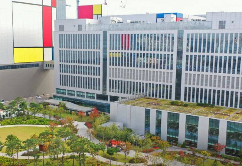
P5 Fab 2 is built for volume
The new facility is slated for a 661-by-194-metre plot, translating to roughly 130,000 square metres, or about 18 football fields. Once equipped for 300 mm wafers, it is expected to handle 200,000 to 300,000 wafers a month, with production spanning memory chips and, potentially, logic components for Samsung Electronics clients.
That scale is the story. P5 Fab 1 and P5 Fab 2 are both three-storey plants, each said to cost about $39 billion. Together they should process 600,000 wafers a month, a number that helps explain why Samsung is pushing the timeline forward rather than waiting for perfect conditions – memory makers rarely get those.
Samsung’s Pyeongtaek build-out keeps expanding
P5 Fab 1 began construction at the end of last year and is due to enter service in 2028. P5 Fab 2 is now expected to start operations in 2029, about half a year earlier than its original construction plan implied. If that schedule holds, Samsung’s total wafer capacity should roughly double by 2029 from the current company-wide level of 650,000 DRAM wafers a month.
- P5 Fab 1 and P5 Fab 2: 600,000 wafers a month combined
- Current Samsung DRAM capacity: 650,000 wafers a month
- P5 Fab 2 output estimate: 200,000 to 300,000 wafers a month
HBM4, NAND and foundry work are all in play
The Pyeongtaek push is only part of the plan. In the existing P4 building, Samsung is installing an extra DRAM line using its sixth-generation 10-nm process, known as 1c, for HBM4 production, with monthly output projected at 100,000 to 200,000 wafers. The company is also ramping 286-layer NAND in China and preparing its Taylor, Texas site for 2 nm chips for Tesla and other customers.
Samsung has also been expanding test and packaging capacity, while promising a substantial increase in capital spending this year without putting a number on the new factories or lines. That leaves one open question: whether this accelerated build-out is enough to keep Samsung ahead in memory, or just enough to stop it from falling behind the rest of the industry.