

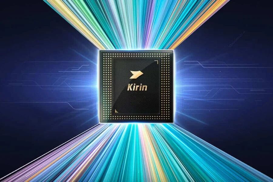
Huawei is betting that the semiconductor industry’s next big leap will come from smarter chip design, not just smaller transistors. At the International Circuit Systems Symposium hosted by the Institute of Electrical and Electronics Engineers, the company introduced what it calls the ”Tau (τ) Law,” a framework it says could help chips reach performance comparable to future 1.4nm processors by 2031 without relying only on the old shrink-everything playbook.
That is a neat pitch, and also a sign of where the industry is stuck. Moore’s Law has spent decades carrying the whole sector on its back, but shrinking nodes now costs more and delivers less dramatic gains. Taiwan Semiconductor Manufacturing Company, Intel, and Samsung all face the same reality: physics still has the final say, and the bill keeps getting uglier.
What Huawei means by Tau Law
Huawei says Tau Law shifts the focus from ”geometric shrinkage” to ”time shrinkage.” In plain English, that means cutting the delay it takes for signals to move around a chip. Less waiting, more work done per second, and, in theory, better efficiency without waiting for the next tiny manufacturing node to save the day.
The company’s answer is something it calls ”logic folding.” Think of it as folding a long, straight road into stacked lanes so traffic gets where it needs to go faster. In chip terms, the aim is to shorten signal paths and squeeze more density out of the same physical space, with Huawei saying the approach spans devices, circuits, chips, and full computing systems.
Kirin 2026 will be the first test
The first commercial chip tied to the idea is expected to be Huawei’s next Kirin 2026 mobile processor, due later this autumn. That makes this more than an academic flex: Huawei wants a real product to carry the claim, not just a symposium presentation and a fancy Greek letter.
He Tingbo, Huawei Semiconductor Business president, said the company has already designed and mass-produced 381 chips over the past six years using ideas linked to the approach. If Huawei can translate that into a visible gain in a consumer phone chip, the rest of the industry will pay attention, even if it does not rush to copy the branding.
- Huawei says Tau Law targets signal delay rather than only transistor shrinkage.
- The company links the approach to ”logic folding” across several chip layers.
- Its first commercial use is expected in the Kirin 2026 mobile chip later this autumn.
- Huawei says the idea could match the density of advanced 1.4nm process technology within the next five years.
How Tau Law compares with Moore’s Law
Huawei also framed the move as a collective problem, saying no single company can solve the semiconductor industry’s bottlenecks alone. That’s sensible, and probably true, because the next phase of chip progress is increasingly about architecture, packaging, and software cooperation as much as it is about lithography. The company’s bigger question now is whether Tau Law becomes a useful engineering model or just another way to describe the industry’s long goodbye to easy scaling.