

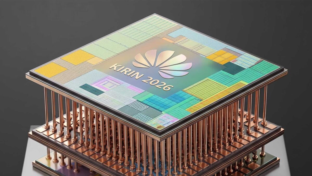
Huawei plans to squeeze more performance from its 7nm Kirin chips-not by moving to a newer fabrication process, but by adopting advanced 3D packaging. According to Chinese sources, the next Kirin lineup will use 3D stacking and hybrid bonding technology, where multiple chip dies are layered vertically and connected through a dense grid of vertical interconnects. For smartphones, this is one of the few practical ways to improve speed and energy efficiency when newer lithography nodes remain out of reach.
Traditionally, key chip components like the CPU, GPU, NPU, and memory are placed side-by-side on a single plane. With 3D stacking, these blocks are arranged in layers on top of each other. This setup shortens data travel distances, reduces latency, cuts power consumption, and boosts bandwidth. The benefits are especially clear in workloads demanding rapid data exchange between compute units-like AI inference and photo or video processing.
For Huawei, this approach is less an experimental leap and more a workaround. US sanctions have restricted the company and its foundry partner SMIC from accessing EUV lithography tools, stalling any push toward 5nm or smaller nodes. Instead, Huawei is fine-tuning the existing 7nm process through architectural tweaks, packaging innovations, and power optimizations. The comeback of the 7nm Kirin 9000s in the Mate 60 Pro last year already demonstrated this strategy.
Huawei isn’t alone in betting on advanced packaging. Industry leaders like TSMC have been developing similar 3D solutions-CoWoS and SoIC-for years. Intel’s Foveros technology and AMD’s multi-die designs in EPYC CPUs and Instinct accelerators follow the same concept. Market analyst Yole Group estimates the advanced packaging market will grow at double-digit rates, exceeding $80 billion by 2030. The reasoning is straightforward: transistor scaling is getting prohibitively expensive, so assembling chips from multiple specialized dies often saves time and money.
Rumors suggest Huawei’s mobile rivals are exploring similar technology. Samsung is reportedly experimenting with more aggressive separation of compute blocks and memory in future Exynos chips, while Apple is believed to be developing even more complex multi-die packaging for upcoming mobile SoCs. The key difference: for Apple and Samsung, this tech mostly adds performance headroom; for Huawei, it’s a chance to narrow the gap created by manufacturing restrictions.
The real challenge is how far Huawei can push this. 3D packaging complicates heat dissipation, demands precise interconnects, and generally increases costs. If Huawei manages to launch mass-produced smartphone SoCs with 3D stacked dies by 2026, it will be one of the clearest examples of the industry seeking performance gains not through smaller process nodes, but through layered chip assembly.