

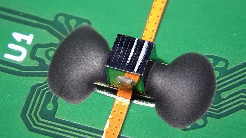
Researchers from Japan and South Korea have unveiled a fresh approach to HBM memory design that could reshape how GPUs and AI accelerators get their data. Instead of stacking DRAM chips vertically in a tower, they suggest positioning these chips on their side to form a dense, volumetric block. The goal: simultaneously tackle bandwidth limits, capacity constraints, and heat buildup-three key bottlenecks holding back high-performance memory.
As AI workloads grow, memory is becoming just as much a choke point as raw compute power. Nvidia’s flagship H100 accelerator, for example, sports up to 80 GB of HBM3 memory, and newer designs push both capacity and bandwidth higher. But cranking up the memory stack height also increases thermal challenges. The higher you build the stack, the harder it is to dissipate heat from the upper layers, trapped between DRAM chips by low-conductivity interposer materials.
Traditional HBM architecture piles DRAM dies atop a base logic chip, linking layers through Through-Silicon Vias (TSVs). This vertical stacking method scaled well for years but is hitting a ceiling. Industry leaders like SK hynix, Samsung, and Micron have pushed HBM to 12- and 16-layer stacks. However, adding each new layer raises costs steeply and worsens thermal load.
At the IEEE VLSI Symposium in June, two alternative memory layouts were presented that turn the stack on its side. These designs ditch the base logic die, giving each DRAM chip its own I/O and power contacts on its ”bottom” edge, allowing direct substrate connections alongside GPUs or AI chips. This sideways approach aims to improve cooling and increase wiring density by sidestepping TSV limitations.
V-Die: flipping the memory stack with microfluidic cooling
The first concept, dubbed V-Die, was developed in collaboration with UNIST and Hanbat National University in South Korea. Researchers not only rotate DRAM dies 90 degrees but embed microfluidic channels between them to pump coolant directly through the memory array. This design promises a substantial drop in operating temperatures and frees up space that TSVs typically occupy.
According to simulations, V-Die achieves roughly four times the number of interconnects compared to upcoming HBM4, cutting read latency by 37%. When tested with a system-level model mimicking a large-scale language model like GPT-3 on Nvidia H100-class hardware, V-Die sustained 540 tokens per second versus 296 tokens per second with traditional HBM4 at equal capacity. Initial token latency dropped by 32%, down to around 24 ms, and temperatures hovered near 45 °C-far cooler than HBM4’s typical peaks above 80 °C under load.
However, the design faces a critical manufacturing hurdle: connecting contacts along the edges of these ”sideways” cubes requires micron-level precision that’s challenging for mass production. Even tiny misalignments can mean defective chips. This precision barrier could restrict V-Die to lab setups unless new fabrication techniques emerge.
MOSAIC: contactless signal transfer for easier assembly
Responding to these challenges, a Japanese team from the University of Tokyo, Tohoku University, and RIKEN proposed a second design called MOSAIC. This approach keeps physical contacts only for power delivery. Data and control signals use contactless inductive coupling via tiny coils etched onto each DRAM chip and corresponding coils on the substrate, aligned perpendicularly to create a magnetic link. This wireless interface relaxes assembly precision requirements considerably.
MOSAIC’s simulations suggest fitting 98 DRAM dies in one cube yields 294 GB of HBM memory. And by thinning DRAM chips down to 100 microns, that number could jump to 294 dies and 882 GB in the same volume. The peak temperature is estimated at 81.3 °C-warm but manageable given the packing density.
Both sideways HBM concepts arrive as the industry grapples with chronic HBM shortages. According to TrendForce, demand for memory in AI systems has outpaced supply for multiple quarters, keeping HBM prices well above regular DRAM. If either V-Die or MOSAIC reaches industrial production, accelerator makers would have new ways to boost HBM memory capacity without endlessly increasing chip area or stack count near the GPU.
The proof, however, will be in working samples integrated with real GPUs and AI chips. With these sideways designs, we may see memory scaling break free from the vertical stack bottleneck that’s long constrained high-performance computing.