TSMC is moving away from mature chip nodes faster than before, and the message to customers is blunt: if you want scale and priority, follow the company toward 4-nm, 2-nm, and beyond. New reports say TSMC 28-nm output has fallen sharply since the start of the year, while the foundry pours more money and equipment into advanced manufacturing, packaging, and silicon photonics.
That is not just a factory reshuffle. It is a profit strategy dressed up as process migration, and it leaves more of the older-node business to rivals such as UMC and VIS. In a market where boring chips still power cars, controllers, and industrial gear, TSMC is choosing the high-margin future over the comfy present.
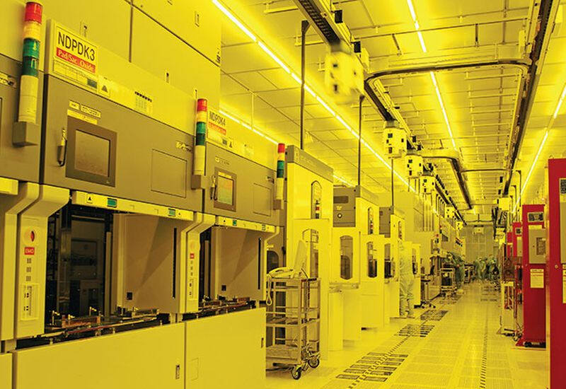
Fab 15A is being converted to 4-nm production
According to Commercial Times, the biggest reduction has hit Fab 15A, where the number of processed wafers with 28-nm chips has dropped by more than 25% since the beginning of the year. The reason is simple enough: the site is being retooled for 4-nm production, and older 28-nm and 22-nm work is being pushed out to make room.
TSMC cannot make 4-nm parts on legacy equipment, so replacement machinery is going in. Nearby Fab 15B remains the company’s main 7-nm site, which makes the split even clearer: mature nodes are being squeezed, while advanced nodes get the best tools and the best economics.
TSMC 28-nm output has fallen to 150,000 wafers a month
At the start of the year, TSMC was producing 200,000 28-nm silicon wafers a month across the facilities suitable for that process. By June, that figure had fallen to 150,000 a month. The decline fits a broader pattern: TSMC wants customers to move from 28-nm to 12-nm where possible, while the company itself keeps scaling up A14, 2-nm, and advanced chip packaging.
- 28-nm output: 200,000 wafers a month at the start of the year.
- 28-nm output: 150,000 wafers a month by June.
- Fab 15A: down more than 25% in 28-nm wafer processing since the start of the year.
- Fab 25: under construction in Taiwan for A14 production.
Older-node work is drifting to UMC and VIS
TSMC is also narrowing what it actually wants to do on 28-nm. The node is increasingly used for substrates in multi-die chips, while discrete logic devices are being made in smaller quantities. That creates room for other foundries, and TSMC’s customers are already turning to UMC and VIS for more of that work.
VIS, which has capital ties to TSMC, is leaning into 200 mm wafer processing now but is building in Singapore around 300 mm infrastructure. That gives it a cleaner path to absorb orders as TSMC reduces its 200 mm footprint. The source says up to 80% of TSMC’s relevant capacity will be handed over to VIS over the next five years, a pretty loud signal that the shift is structural, not a temporary tidy-up.
Fab 25 and the push toward A14
Construction of Fab 25 in Taiwan is also moving quickly, with some work already completed on the P1 building. That facility is expected to host A14 production, reinforcing TSMC’s preference for processes that improve margins and justify heavier investment.
If the current pace holds, TSMC will keep ceding more mature-node volume to competitors while concentrating its own resources on leading-edge chips and packaging. The open question is how far that can go before the older-node business becomes someone else’s market entirely.