Physicists have found that boron-doped diamond does not behave like one neat, uniform superconductor. Instead, tiny superconducting ”pools” form inside it, and those pockets can grow and link together until the material turns into a continuous superconducting network. That odd internal structure could help make future quantum processors easier to build and, just as importantly, easier to connect to ordinary silicon electronics.
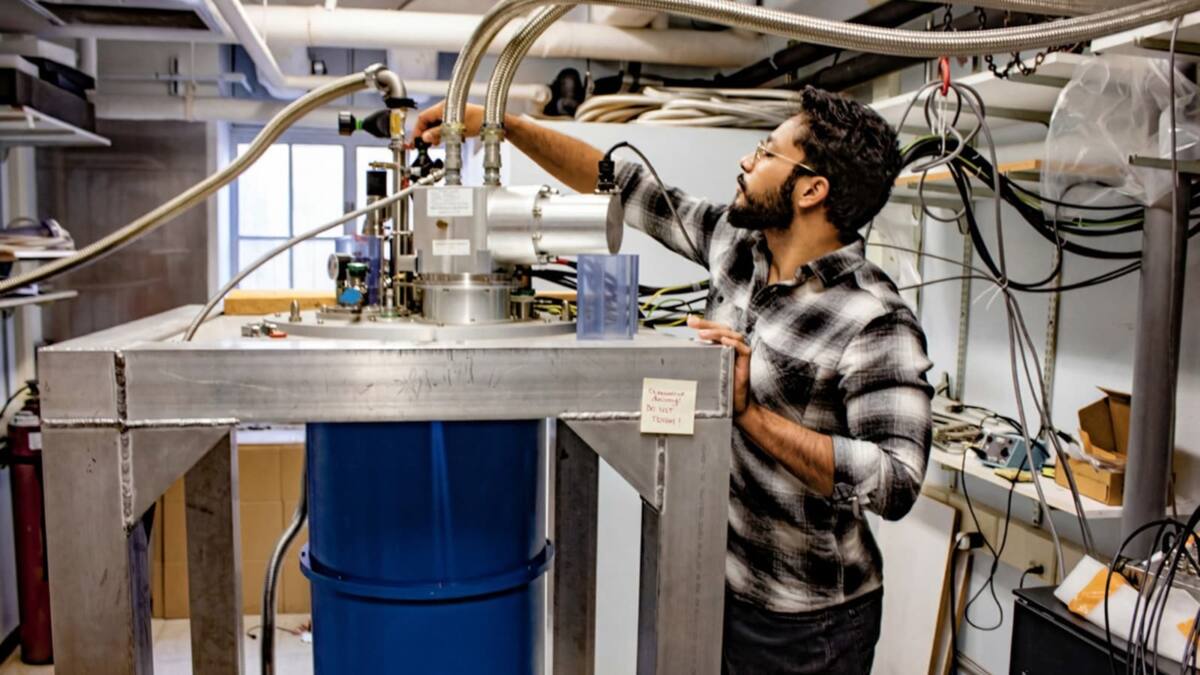
The work comes from researchers at Argonne National Laboratory, Penn State University, and the Pritzker School of Molecular Engineering at the University of Chicago. They studied thin diamond films with boron distributed evenly through the material, then tracked how superconductivity emerged under different conditions. The result is a cleaner explanation for a phenomenon scientists have known about for more than 20 years, but never fully pinned down.
How boron-doped diamond becomes a superconductor
Diamond is famous for being hard and for moving heat with ridiculous efficiency. It is also an electrical insulator unless boron is added, at which point it can carry current without resistance. That transformation has long made boron-doped diamond attractive for advanced electronics, but the missing piece was how the superconducting state actually appears inside the crystal.
The researchers found that the answer is not a perfectly smooth phase change. Microscopic superconducting regions emerge first, then expand and merge as conditions shift. In other words, the material behaves less like a switch and more like a patchwork that gradually fills in.
The knobs researchers can actually turn
Several variables shape those superconducting pockets: temperature, magnetic field, electric current, boron concentration, and the thickness of the diamond film. That matters because it gives engineers a way to tune the material rather than just hope it cooperates. Materials science loves a good surprise, but it loves controllability even more.
- Temperature changes the size and behavior of the superconducting regions.
- Magnetic field and electric current affect how the pockets connect.
- Boron concentration and film thickness also reshape the internal pattern.
A path toward quantum systems on a crystal
The bigger prize is a ”quantum system on a crystal” approach, where one material could host both semiconductor and superconducting behavior. Today, many quantum devices rely on stitching together different materials for classical and quantum functions, which is clever but messy. Diamond could simplify that architecture if researchers can keep these superconducting pools predictable at useful scales.
That would make compact quantum processors, sensors, and other devices more realistic, while also improving compatibility with existing silicon hardware. The catch is that a beautiful lab result is still not a shipping product. The next test is whether these hidden superconducting pockets can be engineered reliably, or whether diamond remains brilliant but stubborn.