

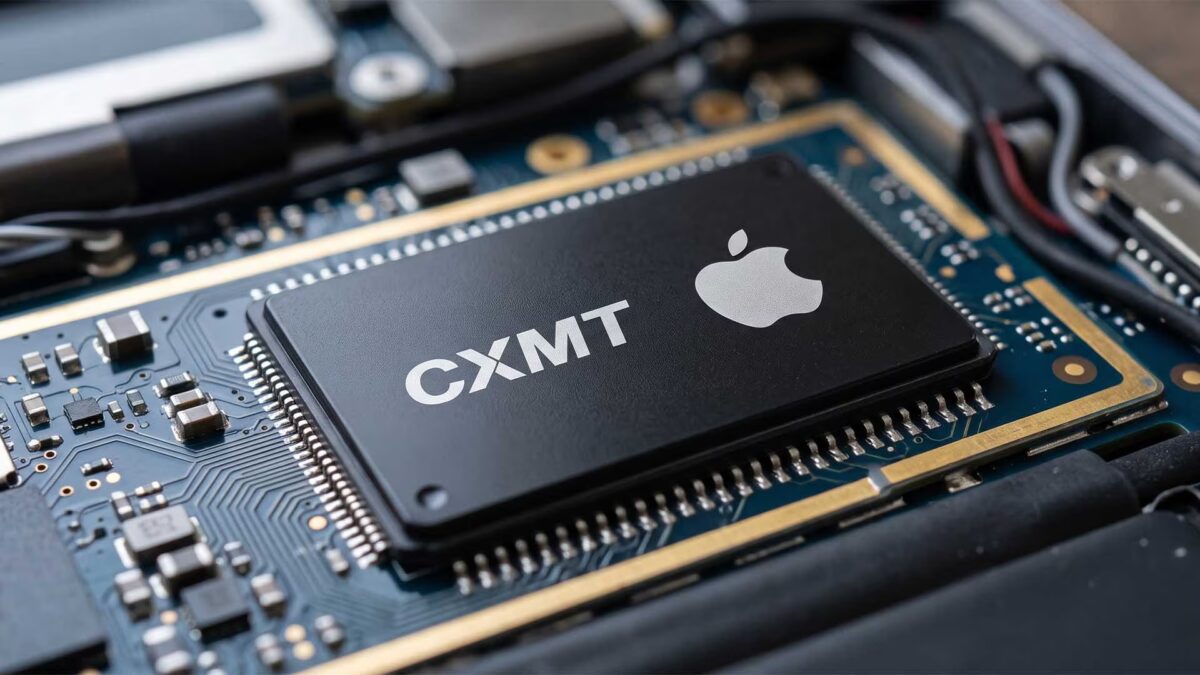
Chinese memory maker CXMT is developing next-gen DRAM using wafer-to-wafer hybrid bonding-a technique that directly bonds two silicon wafers together. This approach aims to boost memory density and speed without relying on EUV lithography, which remains largely inaccessible to Chinese manufacturers. If CXMT can scale this technology to mass production, it could narrow the gap with industry leaders Samsung, SK hynix, and Micron, while positioning itself as a potential new DRAM supplier for Apple.
Unlike conventional DRAM manufacturing that uses micro-bumps to connect circuits, CXMT’s hybrid bonding links two silicon wafers directly. This reduces interconnect length, cutting latency and power consumption, while packing more memory cells into the same chip area. As DRAM faces physical limits in chip packaging-especially with demand surging from AI servers needing faster, larger memory-these efficiency gains are important.
According to sources, CXMT is already testing this wafer-to-wafer bonding method at a pilot line in Hefei, China. They separate the memory cell arrays and control logic onto different wafers, allowing each part to be fabricated using different process nodes. This hybrid process helps avoid pushing the entire chip through expensive, scarce EUV lithography without sacrificing performance.
For China’s semiconductor industry, this isn’t just a neat tweak. Due to a U.S.-led export ban, ASML’s EUV lithography tools are still off-limits to Chinese chipmakers, making advanced DRAM production more difficult and costly. As a result, local companies increasingly turn to packaging innovations, 3D stacking, and hybrid bonding to extract more from available equipment.
How CXMT’s hybrid bonding DRAM differs from conventional memory production
CXMT’s hybrid bonding technique offers several advantages over traditional DRAM manufacturing:
- Direct wafer-to-wafer bonding instead of micro-bumps
- Reduced interconnect length for lower latency and power consumption
- Increased memory density within the same chip footprint
- Separation of memory cell arrays and control logic enables use of different process nodes
- Avoids reliance on costly and scarce EUV lithography tools
The role of hybrid bonding DRAM in China’s semiconductor industry amid EUV bans
The U.S.-led export ban blocks Chinese access to ASML’s EUV lithography machines, forcing semiconductor firms like CXMT to pursue alternative methods for cutting-edge DRAM production. Hybrid bonding, alongside packaging innovations and 3D stacking, has become a key strategy to improve chip performance and yield under these restrictions.
Apple’s interest in CXMT’s hybrid bonding technology
Apple is exploring CXMT as a potential DRAM supplier amid shifting market demands. The memory market now heavily favors AI server applications over traditional consumer electronics like smartphones and laptops. Analysts from TrendForce and Counterpoint report that DRAM prices increased significantly in 2024 and 2025, driven by resource shifts toward more profitable server memory.
- Samsung, SK hynix, and Micron currently dominate global DRAM supply
- Adding CXMT would diversify Apple’s supplier base and reduce risks of shortages
- Apple’s multi-vendor strategy spans displays, storage, modems, and now memory
Until recently, CXMT was viewed primarily as a domestic Chinese supplier rather than a contender for major global device manufacturers. This new technology could change that perception if scaled effectively.
Challenges and outlook for CXMT’s hybrid bonding DRAM
Scaling hybrid bonding DRAM to high yield and stable mass production remains CXMT’s biggest hurdle. Success would mean denser DRAM chips without EUV lithography and competitive costs, enabling CXMT to expand beyond China’s market. Given that the global DRAM industry generates tens of billions annually, securing a large Apple contract could transform this innovation from a pilot test into a major commercial venture.