

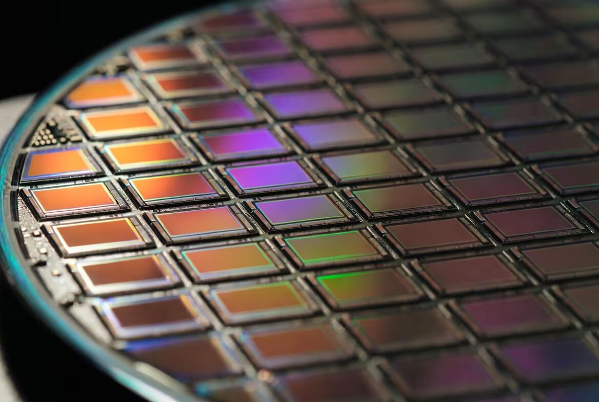
Hangzhou Garen Semiconductor has launched the world’s first commercial production line for homoepitaxial gallium oxide wafers in 6- and 8-inch sizes. The substrate size has long been a bottleneck for gallium oxide adoption. Although the material has generated buzz for years, scaling up to mass production has proven difficult. Garen is already shipping 6-inch wafers to chip developers, with some securing long-term supply contracts.
Gallium oxide is considered one of the most promising materials for next-generation power electronics. Its ultra-wide bandgap-approximately 4.8 to 4.9 eV-and high breakdown electric field enable components to operate at higher voltages and temperatures than silicon-based devices. This unlocks applications in electric vehicles, power grids, energy storage, solar farms, and telecom equipment.
The main challenge has been wafer size. Most gallium oxide devices have been made on 2- to 4-inch substrates, which limits production scale and drives up costs. Hangzhou Garen Semiconductor claims to have developed in-house monocrystal growth and improved epitaxial processes, promising to cut substrate costs by over 80%, reduce iridium consumption, and increase throughput. Their analysis suggests an 8-inch wafer yields roughly four times more chips than a 4-inch one.
For context, the power electronics field is currently dominated by two wide bandgap materials: silicon carbide and gallium nitride. Silicon carbide is widely used in heavy-duty electric vehicle inverters, while gallium nitride has gained footholds in fast chargers, server power supplies, and telecom hubs. Gallium oxide is newer but theoretically supports even higher voltage operation. Moving straight to 6- and 8-inch wafers signals a push to leapfrog laboratory-scale milestones and hit industrial scale faster.
The real test will be how these wafers perform in customer projects. If the 6-inch wafers prove viable, the industry will get its first solid data on defect rates, device longevity, and cost structures for gallium oxide power electronics. Silicon carbide players took years and billions in investment to transition to 8-inch wafers. Gallium oxide now faces the dual challenge of proving its physics advantages can translate into commercial and economic success.