Samsung has restarted work on its 1.4nm foundry process, according to a report, but the company’s timeline is still slipping: mass production is now aimed at 2029, not 2027. That leaves Samsung trailing Intel and TSMC in the race to the next major node shrink, even as it tries to turn recent 2nm progress into a springboard rather than a dead end.
The move suggests Samsung is trying to do two things at once: catch up on advanced logic and avoid repeating the usual foundry trap of chasing the next node before the current one is stable enough to sell. That’s not exactly glamorous, but it is how fabrication businesses avoid expensive embarrassment.
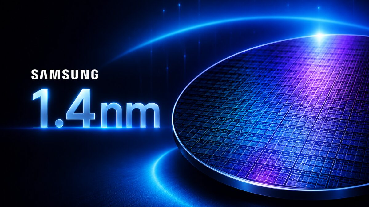
SF 1.4 development is back on the board
The revived process is codenamed SF 1.4, and Samsung has reportedly asked suppliers such as Applied Materials and Lam Research to begin early equipment development. Those tools will first be delivered to NRD-K, Samsung’s semiconductor R&D center, where the company tests its bleeding-edge process work before it ever reaches volume manufacturing.
That matters because equipment lead times are long, and the biggest names in chipmaking usually start pulling those strings years before a node goes live. Samsung’s timing now looks less like a sprint and more like damage control after pushing 1.4nm back to support SF2 and SF2P.
TSMC and Intel still hold the lead
On paper, Samsung still has rivals breathing down its neck. Intel plans to begin mass production of 1.4nm chips in 2027, while TSMC is targeting full-scale production in 2028. Samsung’s 2029 goal puts it one to two years behind, which is not where a top-tier foundry wants to be when customers are deciding who gets the most advanced silicon contracts.
- Intel 14A: mass production planned for 2027
- TSMC A14: full-scale production eyed for 2028
- Samsung SF 1.4: mass production now targeted for 2029
Samsung does have one small edge over TSMC right now: it has already received ASML’s High NA EUV machine at NRD-K, and the tool is expected to be used on select layers starting with 1.4nm. TSMC is still not using high-NA EUV, so Samsung at least gets to wave a genuinely fancy piece of kit around while it tries to close the gap.
The 2nm gamble paid off first
Samsung’s reset makes more sense once you look at the 2nm line. The company reportedly improved yields on SF2 and SF2P and even secured Tesla’s next-generation AI chip business, giving it a reason to slow down and reinforce the current generation before pushing into even more punishing territory.
Samsung is also preparing equipment for its next-generation V12 NAND, which is expected to enter full-scale mass production around 2030. The message is pretty clear: the company wants its foundry and memory roadmaps to move in parallel, because nobody in semiconductors gets rich by pretending one process node can save the whole portfolio.
Samsung’s 1.4nm roadmap before 2029
If Samsung executes cleanly, the gap to Intel and TSMC could narrow by the time SF 1.4 is ready. The bigger question is whether customers will wait that long, or simply lock in their most advanced designs elsewhere and treat Samsung’s comeback as the sequel rather than the premiere.