IBM has sketched out its next leap in chipmaking: a 0.7 nm-class process, or 7 angstroms, built around a three-dimensional NanoStack transistor architecture. The company says the approach should cut power use and lift performance compared with its 2 nm GAA process, and it is aiming to get there no later than 2031.
That is a bold claim, but the direction is sensible. Once chipmakers squeeze conventional layouts hard enough, the next gains tend to come from stacking and smarter packaging rather than simply flattening transistors even further.
From GAA to NanoStack
IBM is not starting from scratch. It is currently working with Japan’s Rapidus on mass production of 2 nm chips using gate-all-around, or GAA, nanowire transistors. That technology itself traces back about 15 years to work IBM did with Samsung before the two companies split paths.
The key shift now is vertical, not just smaller. IBM says NanoStack would place transistors above and beside one another with an offset, taking a cue from CFET-style ideas from Belgium’s IMEC, instead of continuing to compress everything on a single plane.
IBM NanoStack specs and projected gains
According to IBM’s own projections, the 0.7 nm process could deliver up to 50% more performance or as much as 70% better energy efficiency versus its 2 nm GAA process. The company also says SRAM scaling could improve by 40%, which matters because AI accelerators live and die by how close they can keep fast memory to the compute blocks.
- Process class: 0.7 nm, or 7 angstroms
- Target timeline: no later than 2031
- Projected gain: up to 50% more performance or 70% better energy efficiency
- SRAM scaling improvement: 40%
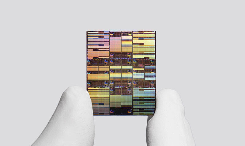
- Planned density: nearly 100 billion transistors on a chip about the size of a fingernail
IBM says the transistors would use channels 15 silicon atoms wide. That kind of atom-count marketing sounds like chipmaking has become a jeweler’s hobby, but it does show how far the industry has moved beyond the old FinFET era.
Why the 3D move matters for AI hardware
The real pressure point is data-center power and cooling. As AI systems grow, moving data back and forth between compute and external memory burns more energy than anyone wants to admit, so denser on-chip memory and better transistor efficiency are becoming a business necessity, not a lab curiosity.
IBM is not alone in chasing that future. IMEC has been pushing CFET-style stacking, and the broader industry has been circling true 3D transistor layouts for years. The difference is that IBM is now putting a date, a density target, and a fairly aggressive efficiency promise on the table.
The race to true 3D chips
For now, the winner is the company that can make the jump from elegant slide-deck architecture to repeatable manufacturing without turning yields into a cautionary tale. If IBM and its partners can pull that off by 2031, the rest of the industry will have a new reference point for what comes after GAA.