Tensordyne, the AI startup formerly known as Recogni, has unveiled Napier, a new AI inference chip built with Broadcom and HPE Juniper Networks that bets on an unusual idea: replace some of the usual multiplication-heavy AI math with simpler logarithmic and addition-based operations, then use that efficiency to squeeze more performance out of far less power. The pitch is blunt enough to get attention in a market where Nvidia’s biggest systems are powerful, expensive, and hungry.
The company says Napier is designed to improve both throughput and cost for large-scale inference, and Tensordyne claims the chip can do that while using 300 W, far below the 1200-W NVIDIA B300 it cites for comparison. That claim will raise eyebrows, naturally, because chip startups love a good efficiency story – but power draw is now one of the main battlegrounds in AI infrastructure, and the winners are increasingly the ones that can deliver tokens without turning a data center into a space heater.
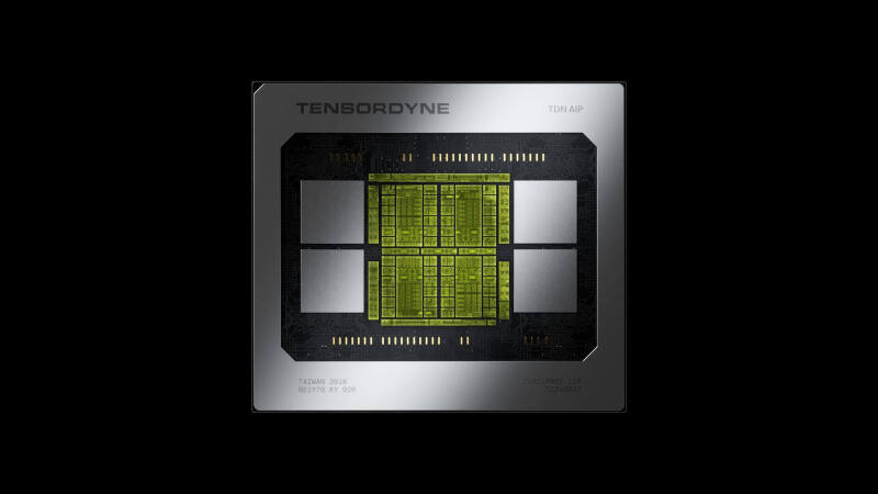
Napier specs and memory layout
Napier’s silicon is packed with 138 billion transistors and supports NVFP4, FP8, and FP16 data modes. Tensordyne says the chip delivers 2.1 petaflops of dense FP8 compute per die, runs its main core at 1.33 GHz, and gives its RISC-V support cores 1.5 GHz. It also includes four HBM blocks, listed by Tensordyne as HBM4 and by ServeTheHome as HBM3E, with 36 GB each for a total of 144 GB and 4.7 TB/s of bandwidth.
There is also a lot of on-chip fast memory: 256 MB of SRAM with 40 TB/s of aggregate bandwidth. That matters because inference engines spend a lot of time waiting on memory, not compute. By pairing a large SRAM pool with HBM, Tensordyne is clearly trying to keep the accelerator fed instead of stalled.
- 138 billion transistors
- 2.1 petaflops FP8 per chip
- 144 GB HBM total
- 256 MB SRAM total
- 300 W claimed power draw
TDN72 rack design and scaling
According to Tensordyne, a 1U node can hold nine TDN chips, plus a 40-core Xeon host CPU, an 8 TB NVMe SSD, two 200GbE QSFP ports, and six TDNLink ports for the company’s own interconnect. One such node is said to deliver 19 petaflops in FP8 mode, along with 1.3 TB of HBM and 2.25 GB of SRAM, while a TDN72 system combines 72 chips across eight nodes.
At the rack level, four TDN72 systems fit into a standard 52U rack, giving 608 petaflops FP8, 42 TB of HBM, 74 GB of SRAM, 256 TB of NVMe storage, 275 TB/s of TDNLink bandwidth, and 64 200GbE ports. Tensordyne says that rack draws just 120 kW and can be cooled with air, which is exactly the sort of claim that makes datacenter operators lean forward and vendors of liquid-cooling gear wince.
The company also says its rack delivers 17 times more tokens per watt and 13 times more tokens per second than a full NVIDIA NVL72 rack, with up to $33 million in additional annual revenue per rack. For very large models, Tensordyne says reaching similar throughput would require at least nine racks of NVIDIA Rubin plus Groq LPX.
Software will decide whether the hardware lands
The biggest risk is not the math block or the memory subsystem. It is software. Tensordyne says it has a model hub on Hugging Face, an SDK, direct compilation for PyTorch and Triton models, and a custom eDSL for Python, all of which sound sensible on paper. But NVIDIA’s real moat is CUDA, plus years of tools, kernels, debugging hooks, and developer habits baked into every serious deployment.
That means Tensordyne is not just selling a chip; it is selling migration friction, or the lack of it. If the company can make Napier easy enough to target, it may find buyers among operators chasing lower cost per token and higher rack density. If not, the spec sheet may end up doing what many bold AI chips do: impressing everyone right up until the software meeting.
The real test will be whether hyperscalers and large inference providers care more about the promised savings than about swapping into a younger ecosystem. If Napier’s efficiency claims hold up in production, expect more noise from the rest of the AI chip field; if they do not, the market will file it under ”interesting architecture” and move on.