TSMC already has ASML’s High-NA EUV tool in-house, but it is in no hurry to put it on the production line. The chipmaker says the machine is being used for research and development, while mass deployment waits for one very unglamorous condition: wafer costs must make sense. In other words, TSMC has High-NA EUV, but it is not rushing into production.
That stance cuts through the lazy narrative that TSMC is simply playing it safe. The company is investing in next-generation lithography, just not blindly, and that is exactly how a foundry that controls so much of advanced chip manufacturing tends to behave. At $380 million to $400 million per machine, High-NA EUV is expensive enough to make even the biggest buyers blink.
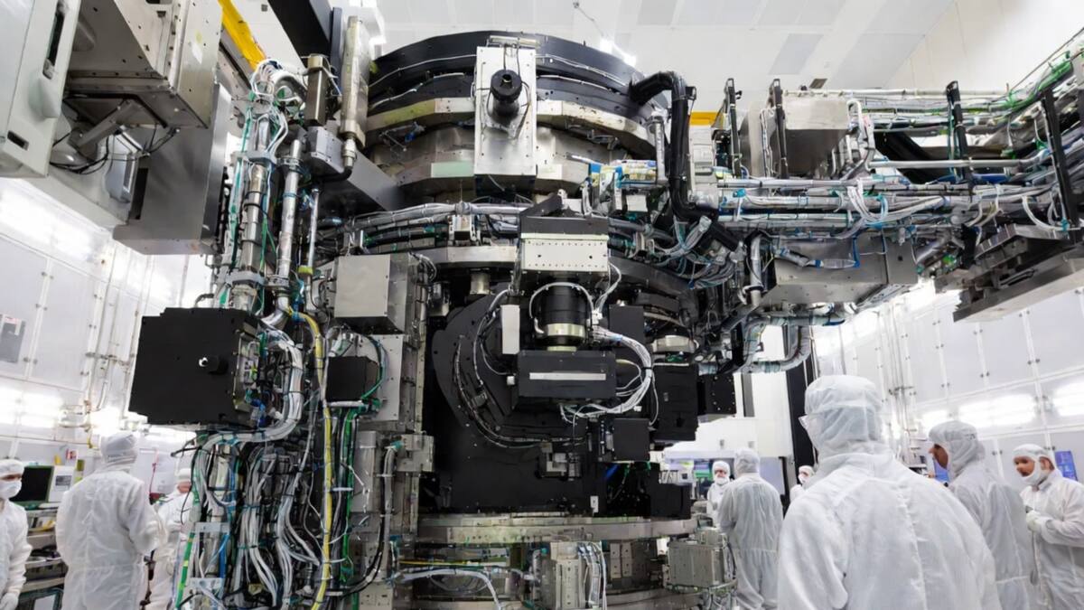
TSMC’s High-NA EUV machine arrived in September 2024
TSMC chairman C.C. Wei told shareholders the company had already purchased a High-NA EUV system, directly rejecting rumors that it was avoiding the technology out of conservatism. The first unit arrived in September 2024 and was installed at TSMC’s research center, where it is being used to develop the lithography process that will eventually support the next generation of chips.
High-NA EUV, or High Numerical Aperture Extreme Ultraviolet, is the toolchain behind the most advanced process nodes, including 2 nm and below. The catch is that the equipment comes with a price tag that is more than twice that of current EUV tools, so the economics have to improve before TSMC scales it up.
Why TSMC is still leaning on current EUV tools
For now, TSMC is prioritizing existing EUV systems to keep miniaturization moving on advanced process technologies. That is the boring answer, but also the sensible one: semiconductor manufacturing is full of sexy new equipment that looks inevitable until someone runs the numbers and discovers the yield math is ugly.
- High-NA EUV cost: $380 million to $400 million per machine
- First TSMC unit received: September 2024
- Current status: research and development, not mass production
- Mass production trigger: competitive wafer costs
ASML still has a customer, just not a stampede
The broader market backdrop matters here. Intel has been more vocal about embracing High-NA earlier in its manufacturing roadmap, while Samsung and TSMC have both shown the usual mix of interest and caution that comes with tools this expensive. No foundry wants to be first into a capital-intensive platform unless the process gains justify the bill.
Even Elon Musk chimed in, saying ASML deserves respect and support and calling it the greatest company in Europe. Flattery is nice, but the real vote of confidence will come when more wafers start flowing through High-NA tools rather than through press releases.
When High-NA EUV moves from lab to fab
The open question is timing. If wafer costs fall enough, TSMC could move quickly because the learning work is already underway. If they do not, High-NA EUV may stay exactly where many bleeding-edge technologies start: impressive, expensive, and stuck in the research lab a little longer than the hype cycle would like.