Huawei says it has designed and mass-produced 381 chips in six years, using that run of silicon to push a homegrown alternative to the industry’s familiar scaling playbook. The company’s pitch is blunt: if US sanctions are meant to block its access to cutting-edge chips, it will keep building around the barriers instead of waiting for them to disappear.
The chips span a wide range of products, from mobile processors and network silicon to base-station chips, automotive control chips, general-purpose computing parts, and AI accelerators. That spread matters because Huawei is not treating this as a one-off research stunt; it is trying to industrialize a methodology that can feed several businesses at once, which is exactly how a constrained supplier stays alive.
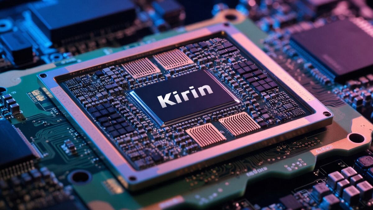
Kirin 2026 and the 382nd chipset
Huawei is also preparing a Kirin 2026 version, due later this year, while framing the 382nd chipset as the next step in its Tau Law roadmap. The company says its high-performance chips should reach transistor density equivalent to 14A, or 1.4 nm, by 2031. That is an audacious target given that leading foundries are still working through 3 nm and 2 nm classes, and it tells you Huawei is leaning hard into roadmap signaling as much as actual product cadence.
- 381 chips designed and mass-produced over six years
- Product lines include Kirin, Ascend AI, network, base-station, and vehicle chips
- Next milestone: the 382nd chipset under the Tau Law approach
- Target for 2031: density equivalent to 14A, or 1.4 nm
LogicFolding and the push for chip independence
Behind the branding, Huawei appears to be building on work from researchers at Peking University, whose 3D design tools were said to underpin the company’s LogicFolding architecture. The broader idea is familiar even if the vocabulary is not: if smaller transistors are harder to obtain, squeeze more out of the design stack, packaging, and layout instead. Intel, TSMC, and Samsung have spent years chasing similar efficiency gains, but Huawei’s version is being sold as a workaround for geopolitical pressure, not just a performance upgrade.
He Tingbo, who leads Huawei’s semiconductor business, argues that the Tau Law points to a new direction for the global chip industry and will eventually be adopted more widely. The claim is ambitious, perhaps predictably so, but Huawei has a reason to keep saying it out loud: sanctions have made technical independence a business requirement, not a slogan. The company has also worked with Chinese researchers on what it calls the world’s first chip for two-dimensional parallel computing, which suggests it is still scattering bets across several architectural ideas rather than waiting for one clean breakthrough.
What Huawei is really betting on
The real story is less about a single chip than about whether Huawei can turn volume, design tricks, and local research into a durable domestic semiconductor stack. If it can keep shipping parts across consumer, networking, industrial, and AI products, it will have something many sanctioned rivals do not: a working feedback loop between theory and revenue. The harder question is whether the rest of the industry will treat Tau Law as a model worth copying, or as a clever detour built for one company’s very specific problems.