A new manufacturing method could help solar panels get better and cheaper at the same time. Researchers from the Karlsruhe Institute of Technology in Germany and the University of Valencia in Spain say they have found a vacuum-based process that forms the perovskite layer in perovskite-silicon tandem cells in about 10 minutes, a big step for a technology that has been promising higher efficiency but has struggled with production speed and cost.
The move matters because conventional silicon panels are getting close to their practical limits, while tandem cells still have room to squeeze more electricity out of the same sunlight. In solar manufacturing, that extra percentage point is rarely glamorous, but it can decide whether a technology stays in the lab or moves onto factory lines.
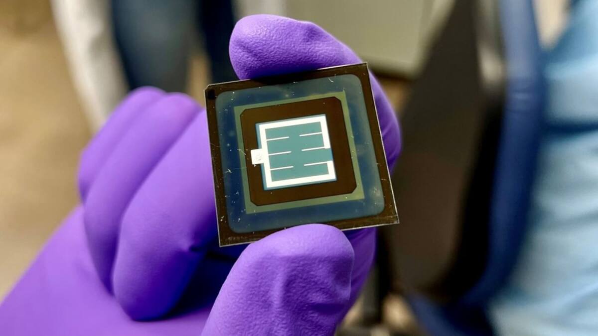
How the vacuum process makes perovskite-silicon tandem cells
Perovskite-silicon tandem cells stack a perovskite layer on top of a standard silicon base. The top layer captures light the lower silicon layer would otherwise miss, which is why these panels can outperform ordinary silicon modules.
The new method uses vacuum deposition: organic materials are evaporated in a vacuum, travel only a few millimeters, and then settle directly onto the silicon wafer as a uniform working layer. That short path sounds almost comically simple compared with the usual industrial headaches around coating, but that is exactly the point.
Just as important, the process is described as flexible enough to work on different kinds of silicon wafers without reconfiguring the equipment. That is the sort of detail manufacturers love, because changing a toolchain for every substrate type is how good ideas get stuck in pilot production forever.
Perovskite-silicon tandem cell efficiency on different wafers
In testing, the new solar cells reached 23.5% on smooth wafers, 23.7% on nanostructured wafers, and up to 24.3% on industrial textured wafers. For a young production method, that is a strong showing, especially because it demonstrates the technique can hold up outside ideal laboratory conditions.
- 23.5% on smooth wafers
- 23.7% on nanostructured wafers
- 24.3% on industrial textured wafers
The broader backdrop is obvious: solar makers are hunting for upgrades that raise output without forcing a painful reset of factories and supply chains. Tandem cells are one of the clearest paths forward, and the more closely the process resembles standard industrial methods, the more likely it is to survive the journey from research paper to production.
Lower material use could help mass production
The researchers also say the process uses fewer expensive materials and allows some components to be reused. That is not just a nice sustainability flourish; in solar manufacturing, shaving material costs can matter as much as improving efficiency, because the cheapest watt tends to win.
If the method scales as advertised, it could give manufacturers a faster and cheaper way to produce next-generation panels with better performance than mainstream silicon products. The real test now is whether this 10-minute process can keep its numbers when it leaves the carefully controlled world of the lab and meets industrial volume.